Objectives
In this experiment, you will study the current-voltage ( I-V ) characteristics of semiconductor diodes (silicon diode, germanium diode).
Apparatus
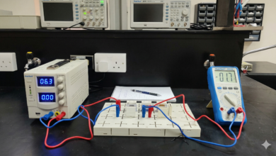
1- Breadboard or Rastered socket panel, DIN A4.
2-DC Power Supply.
3- DC Voltmeter.
4- DC Ammeter.
5- Si diode (1N4007).
6- Ge diode (AA118).
7- Resistor 100Ω.
8- Connecting wires.
9- Set of bridge plugs.
Theory
Virtually all aspects of electronic circuit technology rely on semiconductor
components. The semiconductor diodes are among the simplest of these. They consist
of a semiconductor crystal in which an n-conducting zone is adjacent to a pconducting zone. Capture of the charge carriers, i.e. the electrons in the n-conducting and the “holes” in the p-conducting zones, forms a low conductivity zone at the junction called the depletion layer. The size of this zone is increased when electrons or holes are removed from the depletion layer by an external electric field with a certain
orientation. The direction of this electric field is called the reverse direction. Reversing
the electric field drives the respective charge carriers into the depletion layer, allowing
current to flow more easily through the diode.
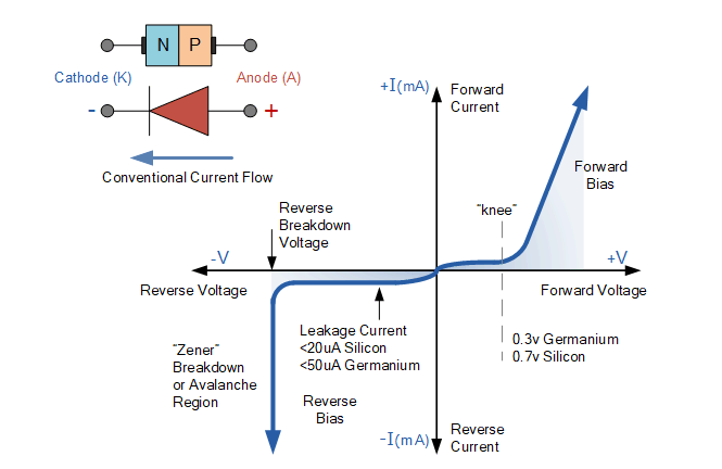
In this experiment, the current-voltage characteristics of an Si-diode (silicon diode)
and a Ge-diode (germanium diode) diode are measured and graphed manually point by
point. The aim is to compare the current in the reverse direction and the threshold
voltage as the most important specifications of the two diodes.
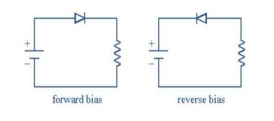
Forward Bias:
The voltage is connected positive, (+v) to the P-type material and negative, (-v) to the N-type material across the diode which has the effect of decreasing the PN-junction width.
Reverse Bias:
The voltage is connected negative, (-v) to the P-type material and positive, (+v) to the N-type material across the diode which has the effect of increasing the PN-junction width
Procedure
PART A: Silicon pn junction diode:
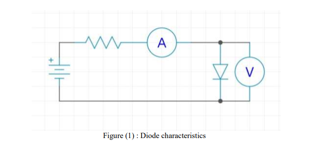
1- Connect the circuit (Forward Bias) as shown in figure (1), the power supply is
set to zero volts.
2- Vary the forward voltage (Vf) and observe the forward current (If).
3- Measure and record in table (1).
4- Reverse the diode in the circuit of Figure (l), (Reverse Bias).
5- Vary the Reverse voltage (Vr) and observe the Reverse current (Ir).
6- Measure and record in table (1)
7- Plot the I-V curve: the current (Y-axis) versus the voltage (X-axis).
8- Determine the forward resistance Rf and threshold voltage Vth
PART B: Germanium pn junction diode:
1- Repeat the above measurements using Ge diode.
2- Measure and record in table (2).
3- Plot the I-V curve: the current (Y-axis) versus the voltage (X-axis).
4- Determine the forward resistance Rf and threshold voltage Vth
Circuit Diagram
Data Sheet
Si diode (1N4007)
| (mA) Ir | (V) Vr | (mA) If | (V) Vf |
|---|---|---|---|
Ge diode (AA118)
| (mA) Ir | (V) Vr | (mA) If | (V) Vf |
|---|---|---|---|